Color Blasted Badge Making: How Hard Could It Be
Abhinav Panda, Bradán Lane
DEF CON 32 Creator Stage · Day 1 · Creator Stage
Overview
This talk, presented at DEF CON 32, dives into the intricate and often challenging world of creating full-color, custom printed circuit board (PCB) badges. Abhinav Panda, a veteran of the "badge life" community, and Braden Lane, a hardware hacker and UX designer, share their extensive experimentation and hard-won knowledge on two primary methods: UV printing and traditional silk screening. The talk explores the technical processes, practical considerations, and unique challenges associated with transforming standard PCBs into vibrant, artistic, and functional conference badges.
Key moments
- 0:00 Talk introduction and UV printing overview
- 1:15 Origin story: First UV printed badge (RSA)
- 2:55 Detailed UV printing process and alignment solution
- 4:00 Challenges: Reflow issues and UV printer maintenance
- 5:25 Braden Lane introduces screen printing as alternative
- 6:45 Hamster's perspective on hacking PCB manufacturing
Color Blasted Badge Making: How Hard Could It Be
Speakers: Abhinav Panda, Braden Lane
Conference: DEF CON 32
YouTube: https://www.youtube.com/watch?v=q1Uap5uinIo
Overview
This talk, presented at DEF CON 32, dives into the intricate and often challenging world of creating full-color, custom printed circuit board (PCB) badges. Abhinav Panda, a veteran of the "badge life" community, and Braden Lane, a hardware hacker and UX designer, share their extensive experimentation and hard-won knowledge on two primary methods: UV printing and traditional silk screening. The talk explores the technical processes, practical considerations, and unique challenges associated with transforming standard PCBs into vibrant, artistic, and functional conference badges.
The discussion highlights the journey from conventional, often monochromatic, PCB designs to highly customized, visually rich artifacts that have become a hallmark of hacker conferences. Panda details his eight-year odyssey with UV printing, from its initial application as a solution for a specific color requirement to establishing a dedicated "badge life lab." Lane complements this by presenting traditional silk screening as a robust alternative, particularly for its tolerance to the manufacturing process. This session is crucial for anyone interested in the intersection of hardware, art, and community, offering valuable insights into pushing the boundaries of PCB fabrication for creative expression.
Background
▶ Watch: Talk introduction and UV printing overview (0:00)
The "badge life" phenomenon within the hacker community has evolved significantly, transforming conference badges from simple identification cards into complex, often interactive, electronic art pieces. Historically, PCBs were primarily functional components, typically green with white silkscreened legends. Achieving intricate, multi-color designs on these boards presented considerable challenges due to the limitations of standard PCB manufacturing processes. Traditional screen printing, while effective for basic graphics and text, struggled with precise color matching and fine details, especially when dealing with specific brand colors or complex artwork.
The speakers illustrate this challenge with a specific anecdote: their early attempts to replicate a unique shade of pink for an RSA conference badge using standard screen printing methods proved unsuccessful. This limitation sparked their quest for alternative techniques, leading them to explore methods beyond conventional PCB fabrication. The desire to imbue badges with greater artistic complexity, incorporating full-color graphics, gemstones, and even gold plating, necessitated innovative approaches to printing directly onto the PCB substrate. This drive for unique, visually striking badges, often pushing the boundaries of what manufacturing fabs typically expect, forms the core impetus for the techniques discussed in this talk.
Key Findings
▶ Watch: Detailed UV printing process and alignment solution (2:55)
The talk presents several key findings and insights derived from extensive practical experimentation in advanced badge manufacturing:
- UV Printing for Full-Color Fidelity: UV printing emerges as a highly effective method for achieving full-color, high-resolution graphics directly onto PCBs, overcoming the limitations of traditional screen printing for specific color matching and intricate designs. It allows for printing on a wide array of materials, including components themselves.
- Alignment is Critical and Challenging: Precise alignment of the PCB under the printer head is paramount for successful UV printing. The speakers developed a two-step process involving printing a registration layer on the printer bed first, followed by manual PCB alignment, to mitigate common alignment issues.
- Post-Printing Assembly Challenges: While hand soldering is generally unaffected by UV printed layers, reflow oven processes pose a significant challenge. The heat from reflow can cause UV-cured ink to yellow or lose its original shade, necessitating extensive experimentation with color correction and temperature profiles for each unique design.
- High Maintenance for UV Printers: UV printers require consistent operation to remain functional. Daily printing is recommended to prevent ink clogging and maintain the health of the print head, indicating a significant operational overhead for hobbyists or small-scale producers.
- Screen Printing as a Reflow-Tolerant Alternative: Traditional silk screening, utilizing actual PCB solder mask ink, offers a robust solution for designs that require high tolerance to reflow soldering processes. This method ensures the printed layer withstands assembly temperatures without degradation, albeit with potential limitations in color fidelity and finish variability compared to UV printing.
- Artistic Material Integration: Both methods facilitate the integration of diverse materials and unique ideas into badge designs, such as gemstones and gold plating, pushing the aesthetic and tactile boundaries of conference badges.
Technical Deep Dive
▶ Watch: Challenges: Reflow issues and UV printer maintenance (4:00)
The talk delves into the technical intricacies of two distinct approaches to achieving full-color and enhanced aesthetics on PCBs: UV printing and traditional silk screening.
UV Printing: Abhinav Panda's Approach
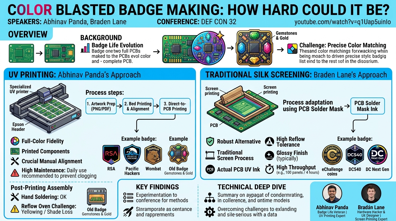
Abhinav Panda's primary technique revolves around UV printing, a method he has refined over eight years of "badge life" experimentation. UV printing utilizes ultraviolet light to instantly cure inks as they are jetted onto a substrate. This technology is widely used for printing on various materials like banners, acrylic, and phone cases, but its application to PCBs, especially for artistic purposes, involves unique challenges and adaptations.
Panda's setup involves a dedicated UV printer, which visually resembles a flatbed printer with a print head that traverses back and forth across a printing bed. The specific machine used by Panda's lab is their second iteration, described as a local brand customized with an Epson header. This choice reflects the high cost of large-scale commercial UV printers, making custom or locally sourced solutions more accessible for specialized applications like badge making. The printer bed measures approximately 2 feet by 3 feet, capable of accommodating 60 to 70 badges per run, with an average print time of roughly one minute per badge.
The printing process involves several critical steps:
- Artwork Preparation: Designs, typically in PNG or PDF format, are loaded into the printer's proprietary software.
- Bed Printing and Alignment: To achieve precise alignment, a common challenge with UV printing, Panda's team employs a clever two-phase strategy. First, a registration layer or an outline of the artwork is printed directly onto the printer's bed. Second, each individual PCB is then manually aligned on top of this printed layer. This manual alignment ensures that the subsequent full-color print accurately registers onto the PCB.
- Direct-to-PCB Printing: Once aligned, the UV printer applies the full-color design directly onto the PCB surface. The UV light then immediately cures the ink, resulting in a durable, vibrant print.
Panda highlighted several practical considerations and challenges:
- Impact on Components: When printing on assembled badges (PCBs with components already soldered), the UV ink layer can inadvertently cover and color the electronic components themselves. While this might be aesthetically interesting, it could potentially impact component visibility or thermal properties, though the talk doesn't elaborate on functional issues.
- Soldering Compatibility: Hand soldering after UV printing poses no significant issues, indicating that the cured UV ink can withstand localized heat without degradation.
- Reflow Oven Sensitivity: The reflow oven process, common in surface-mount technology (SMT) assembly, presents a major hurdle. The high temperatures inside a reflow oven can cause the UV-printed layer to turn yellowish or lose its original color shade. This necessitates extensive experimentation with shades for color correction and refining reflow profiles to find a "sweet spot" that preserves the desired aesthetics. This trial-and-error process is often unique to each design and badge material.
- Printer Maintenance: UV printers are described as high-maintenance machines. To prevent ink clogging and keep the print head healthy, it's crucial to operate them regularly, ideally printing something every day.
Panda showcased various examples of successful UV-printed badges, including the RSA badge (their first UV-printed badge, solving a specific pink color requirement), a Pacific Hackers badge, a Wombat badge from B-Sides Adelaide, and an "old badge" featuring a combination of gemstones and gold plating, demonstrating the technique's versatility for integrating diverse materials.
Traditional Silk Screening: Braden Lane's Approach
Braden Lane presents traditional silk screening as an alternative, particularly motivated by the challenges of UV printing with respect to reflow processes. Lane recognized that solder mask ink, a material inherently tolerant to reflow temperatures, could be adapted for artistic printing. His method leverages the same principles used for printing t-shirts, but applied to PCBs.
Key aspects of Lane's silk screening technique include:
- Reflow Tolerance: The primary advantage of using actual PCB UV ink (similar to solder mask) is its inherent ability to withstand the high temperatures of a reflow oven without discoloration or degradation, a stark contrast to the issues encountered with general UV printing inks.
- Process Adaptation: Lane applies the entire traditional silk screening process, which involves creating a stencil (screen) for each color and then pushing ink through the stencil onto the PCB. This is an "old school classic" method, adapted for the precision required for PCBs.
- Ink Type: He explicitly states using "actual PCB UV ink," ensuring compatibility with standard PCB manufacturing processes and durability.
- Finish Characteristics: The finish achieved with silk screening using PCB UV ink is generally glossy, similar to the standard solder mask and silkscreen layers found on commercially manufactured PCBs. While it's theoretically possible to add a matting agent to achieve a matte finish, Lane notes that in his context, which he describes as "more art than science," the finish can be variable.
- Throughput: Lane mentions a significant throughput for his manual process, achieving approximately 100 panels in about four hours, demonstrating its viability for batch production.
Both speakers emphasize continuous experimentation to discover new materials, techniques, and solutions, pushing the boundaries of what's achievable in custom PCB badge design.
Demo / Proof of Concept
▶ Watch: Braden Lane introduces screen printing as alternative (5:25)
While the talk did not feature a live, step-by-step demonstration of the UV printing or screen printing process in action, the speakers presented numerous physical examples of their finished badges as robust proof-of-concept for their techniques. These artifacts served to visually validate the capabilities of both UV printing and traditional silk screening for creating intricate, full-color, and multi-material PCB designs.
Abhinav Panda showcased a range of UV-printed badges:
- RSA Badge: This was highlighted as their inaugural UV-printed badge, specifically created to accurately reproduce a unique shade of pink in the conference logo that traditional screen printing could not achieve. This served as the catalyst for their deep dive into UV printing.
- Pacific Hackers Badge: An example demonstrating the application of UV printing for a community in Silicon Valley, likely featuring complex graphics.
- Wombat Badge from B-Sides Adelaide: Another instance illustrating the global reach and artistic versatility of their methods.
- "Old Badge" with Gemstones and Gold Plating: This particular badge was a standout example, combining a gold-plated PCB with embedded gemstones. Panda emphasized the significant manual effort involved in integrating such diverse materials, showcasing the extent to which they push the boundaries of badge design beyond mere printing.
Braden Lane's contribution, while not detailing specific badge examples in the same way, implicitly demonstrated the effectiveness of traditional silk screening through his consistent production for entities like eChallenge coins, DC540, and DC Next Gen. The core proof of concept for Lane's method lies in its ability to produce reflow-tolerant, durable printed layers using standard PCB UV ink, making it a reliable choice for designs requiring integration into standard electronics assembly flows. The visual quality and durability of these badges, as presented and discussed, serve as the primary evidence of the successful application of their respective techniques.
Defensive Implications
▶ Watch: Hamster's perspective on hacking PCB manufacturing (6:45)
While this talk primarily focuses on the artistic and manufacturing aspects of badge creation rather than cybersecurity vulnerabilities, the insights shared have significant implications for how conference badges are designed, secured, and perceived, particularly within the context of physical security and identity.
For badge creators and organizers, understanding these advanced printing techniques offers opportunities:
- Enhanced Authenticity and Anti-Counterfeiting: The ability to produce highly complex, full-color, and multi-material designs through UV printing and screen printing can significantly increase the difficulty of counterfeiting conference badges. Unique color schemes, intricate patterns, and the integration of non-standard materials like gemstones or gold plating can act as physical security features, making replication by unauthorized parties much harder without specialized equipment and expertise.
- Brand Integrity and Recognition: Accurate color reproduction, particularly critical for conference logos and branding (as demonstrated by the RSA badge example), ensures that badges consistently represent the conference's identity. This attention to detail can enhance the perceived professionalism and value of the event.
- Durability and Longevity: The choice of printing method impacts the badge's durability. While UV printing offers vibrant colors, its sensitivity to reflow oven temperatures means that post-assembly printing or careful process control is necessary. Conversely, screen printing with solder mask ink provides a highly robust and reflow-tolerant finish, ideal for badges intended to withstand environmental factors or extensive handling.
- Supply Chain Considerations: The technical challenges, such as UV printer maintenance and the need for manual alignment, highlight the complexities of producing these badges. Organizations commissioning custom badges must factor in these specialized requirements, potentially opting for providers with specific expertise or in-house capabilities, like Panda's proposed "UV Printing and PCBA service at Hackerware." This impacts cost, lead time, and the overall reliability of the badge supply chain.
- Forensic Analysis of Badges: For security researchers or event staff, understanding the characteristics of these printing methods can aid in the forensic analysis of badges. For instance, the specific yellowing or shade loss observed in UV-printed badges after reflow could be a recognizable characteristic, helping to identify manufacturing processes or potential modifications.
In essence, while not directly addressing software vulnerabilities or network defense, the talk equips badge designers and event organizers with the knowledge to create more secure, aesthetically appealing, and durable physical credentials, contributing to the overall integrity of a conference's physical environment and brand.
Key Takeaways
- UV Printing Offers Unprecedented Color Fidelity: UV printing allows for full-color, high-resolution graphics directly onto PCBs, ideal for complex designs and precise brand color matching that traditional screen printing struggles with.
- Alignment and Reflow are Major UV Printing Challenges: Achieving accurate alignment requires specialized techniques like printing a registration layer, and UV-cured inks are susceptible to yellowing or shade loss during reflow oven processes, demanding extensive experimentation.
- Screen Printing Provides Reflow Robustness: Traditional silk screening using actual PCB UV ink (solder mask ink) is highly tolerant to reflow temperatures, making it a durable choice for designs where post-assembly integrity is crucial.
- Badge Making is High-Effort Experimentation: Both methods require significant experimentation with materials, processes, and equipment (e.g., UV printer maintenance, color correction for reflow) to achieve desired artistic and functional outcomes.
- Diverse Material Integration is Possible: Advanced techniques enable the incorporation of unique materials like gemstones and gold plating directly onto PCBs, elevating badges from functional electronics to intricate art pieces.
- Consider Manufacturing Workflow: The choice between UV printing and screen printing should be guided by design complexity, required color accuracy, budget, desired durability, and the assembly process (e.g., pre-assembled vs. post-assembly printing).
About the Speaker(s)
Abhinav Panda (also known as "Panda") is a prominent figure in the "badge life" community, with eight years of dedicated experience in custom badge creation. His journey began serendipitously while attempting to make badges for an Indian conference, quickly developing into a passion for pushing the boundaries of PCB artistry. Over time, he has established his own "badge life lab" equipped with specialized machinery for fabrication, where he conducts "crazy weird experiments with crazy failures and crazy successes." Panda is an expert in UV printing for full-color badge making, a technique he pioneered for conference badges after realizing its potential to print on "anything" to achieve specific color requirements. He is contemplating starting a UV Printing and PCBA service at Hackerware in the future.
Bradán Lane (also known as "Braden Lane") is a UX designer and user researcher with a strong passion for hardware hacking, despite having no formal training in the field. He has contributed significantly to the badge community through his work on eChallenge coins, and for groups like DC540 and DC Next Gen. Lane's expertise lies in applying traditional silk screening methods to PCBs, a technique he chose for its inherent tolerance to the reflow process, utilizing actual PCB UV ink. His approach emphasizes the practicality and robustness of classic printing methods for creating durable and visually appealing hardware art.