Nano Enigma Uncovering the Secrets in eFuse Memories
Michal Grygarek, Martin Petr
DEF CON 32 Main Stage · Day 1 · Main Stage
Overview
In the realm of embedded system security, hardware-based protections are often considered the strongest line of defense. Among these, eFuse memories play a critical role, serving as one-time programmable (OTP) storage for immutable configurations such as secure boot keys, debugging interface disablements, and device unique identifiers. However, a talk presented at DEF CON 32 by Martin Petr and Michal Grygarek, titled "Nano Enigma: Uncovering the Secrets in eFuse Memories," challenged a fundamental assumption underlying the confidentiality of data stored in these eFuses.
Key moments
- 0:00 Introduction to eFuses and their security applications
- 2:30 Proving delayering is feasible on ESP32
- 4:10 Overview of chip decapsulation methods
- 5:00 Chosen chemical decapsulation method explained
- 6:20 Exploring various chip delayering techniques
- 8:00 Practical mechanical delayering with a wet stone
Nano Enigma Uncovering the Secrets in eFuse Memories
Speakers: Michal Grygarek, Martin Petr
Conference: DEF CON 32
YouTube: https://www.youtube.com/watch?v=z33TSv9EXBQ
Overview
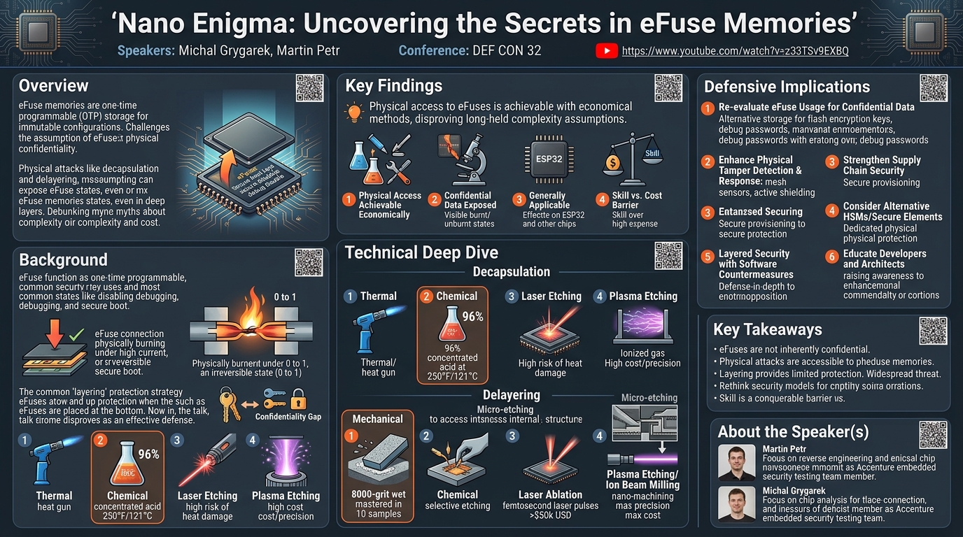
In the realm of embedded system security, hardware-based protections are often considered the strongest line of defense. Among these, eFuse memories play a critical role, serving as one-time programmable (OTP) storage for immutable configurations such as secure boot keys, debugging interface disablements, and device unique identifiers. However, a talk presented at DEF CON 32 by Martin Petr and Michal Grygarek, titled "Nano Enigma: Uncovering the Secrets in eFuse Memories," challenged a fundamental assumption underlying the confidentiality of data stored in these eFuses.
The speakers, members of Accenture's embedded system security testing team in Prague, demonstrated that physical attacks, specifically decapsulation and delayering, can be performed with accessible tools and techniques, effectively exposing the "burnt" or "unburnt" state of individual eFuses. This talk is significant because it debunks the long-held belief that such physical attacks are prohibitively complex and expensive, particularly when eFuses are situated in the deepest layers of a chip as a supposed protection measure. Their work serves as a stark reminder that physical access to a device can compromise even seemingly robust hardware security mechanisms, urging manufacturers and developers to reconsider their reliance on eFuses for storing highly confidential data like flash encryption keys or debug passwords.
Background
▶ Watch: Introduction to eFuses and their security applications (0:00)
eFuses are fundamental electronic components designed for permanent, one-time programmable changes within integrated circuits. Conceptually, an eFuse is a simple connection that, when subjected to a current exceeding a specific threshold, physically "burns" or terminates, changing its electrical state irreversibly. This property makes eFuses ideal for implementing one-time programmable (OTP) memory, where a bit's state can be changed from zero to one, but never back to zero. This permanence is invaluable for various security-critical functions in embedded systems.
Manufacturers widely leverage eFuses for several key security purposes. For instance, they can be used to permanently disable debugging interfaces (like JTAG or SWD) after device manufacturing, preventing unauthorized access to internal states and data. They also play a crucial role in enabling secure boot mechanisms by storing public keys or hashes of trusted bootloaders, ensuring only authenticated firmware can execute. However, as highlighted by the speakers, some manufacturers have extended this use case to store information requiring confidentiality protection. This includes highly sensitive data such as flash memory encryption keys or passwords for debugging interfaces. The critical issue arises because the "burnt" or "unburnt" state of an eFuse is a physical characteristic, directly observable under a microscope.
To address this inherent vulnerability, a common protection measure employed by chip designers is layering. In chip manufacturing, components are stacked in multiple layers. By placing the eFuse-based memory in the very bottom layer of the silicon die, manufacturers assume that direct observation is extremely difficult. This protection strategy is predicated on the assumption that the process of delayering – carefully removing the overlying material layers to expose the eFuses – is a highly complex, time-consuming, and prohibitively expensive endeavor, requiring specialized equipment and expertise typically only available to state-sponsored actors or well-funded industrial labs. The "Nano Enigma" talk directly challenges and disproves this assumption, demonstrating that these physical attacks are far more accessible than commonly believed.
Key Findings
▶ Watch: Overview of chip decapsulation methods (4:10)
The central and most significant finding presented in "Nano Enigma" is the successful debunking of the assumption that delayering and physical observation of eFuse memories are prohibitively complex and expensive for many adversaries. The speakers effectively demonstrated that, with a combination of readily available tools and acquired skills, it is possible to physically access and observe the state of eFuses, even when they are intentionally placed in the deepest layers of a chip for confidentiality protection.
Specifically, their work revealed that:
- Physical access to eFuses is achievable with economical methods: The team showcased techniques for both decapsulation (removing the chip's epoxy housing) and delayering (etching away silicon layers) that do not require multi-million dollar equipment. They achieved success using chemical methods for decapsulation and mechanical methods for delayering, keeping the cost significantly lower than high-end laser or plasma alternatives.
- Confidential data stored in eFuses can be exposed: By successfully preparing the chip, the physical state of the eFuses (burnt or unburnt) becomes visible under a microscope, allowing an attacker to read out sensitive information such as flash encryption keys or debug interface passwords. This directly undermines the confidentiality claims made for such data.
- General applicability to a wide range of chips: While the demonstrations were performed on an ESP32 chip from Espressif, the speakers emphasized that the methodologies and underlying principles are generally applicable to virtually any chip utilizing eFuse-based memories. This implies a widespread vulnerability across various embedded systems that rely on eFuses for storing confidential, rather than merely immutable, data.
- Skill, not just cost, is the primary barrier: The talk highlighted that while precision and patience are required, the necessary skills for mechanical delayering can be "mastered" within a reasonable number of attempts (e.g., 10 samples), suggesting that the barrier to entry is lower than often perceived for determined attackers.
These findings collectively represent a critical security revelation for the embedded systems industry, indicating that the physical security of eFuse-stored secrets needs to be re-evaluated, and alternative or supplementary protective measures should be considered.
Technical Deep Dive
▶ Watch: Chosen chemical decapsulation method explained (5:00)
The technical core of the "Nano Enigma" talk revolved around the detailed methodology for physically accessing and analyzing eFuse memories. This involved two primary stages: decapsulation and delayering, each presenting its own set of challenges and requiring specific techniques. The speakers meticulously outlined various approaches for both, ultimately detailing their chosen, cost-effective methods.
Decapsulation: Removing the Chip's Housing
Decapsulation is the initial step, involving the removal of the chip's protective epoxy housing to expose the bare silicon die. The speakers discussed four primary techniques for this:
- Thermal Method: This involves heating the epoxy housing, typically with a blue torch or heat gun, and then carefully breaking it to extract the silicon plate. While simple and inexpensive, it lacks precision and can be risky.
- Chemical Decapsulation: This method uses concentrated chemicals, specifically strong acids, to dissolve the epoxy housing. The speakers chose this method due to its "availability and good reliability." They specified using 96% concentrated acid, heated to approximately 250 degrees Fahrenheit (121 degrees Celsius). This process can be combined with laser ablation to first remove a large portion of the housing, reducing the chip's exposure time to the acid and minimizing potential damage.
- Laser Etching: This technique employs a strong laser beam to vaporize the epoxy material. The primary risk associated with laser etching is the potential for heat deposition into the sample, which can easily burn the delicate silicon plate, rendering the chip useless.
- Plasma Etching: This advanced process involves ionized gas (plasma) for selective etching of materials. While offering high precision, it typically comes with a significantly higher price tag and complexity.
For their practical demonstrations, the team primarily relied on chemical decapsulation due to its balance of effectiveness and accessibility.
Delayering: Accessing the Internal Structures
Once the silicon die is exposed, the next critical step is delayering. This process involves carefully removing the metallization and dielectric layers that sit atop the eFuse memory, which is often located in the very bottom layers of the chip. Without delayering, the internal structures, including the eFuses, remain obscured. Again, four main approaches were presented:
- Mechanical Delayering: This is the most cost-effective method, starting at around $100. It involves physically grinding or polishing the chip's surface. The speakers specifically detailed their use of a wet stone with a very high 8000 grit size. This technique requires considerable skill and patience; as Michal Grygarek noted, he personally "mastered it around 10 samples." Too much pressure can quickly damage the underlying structures, necessitating a restart. With careful, systematic polishing, a beautiful etched chip can be obtained within 30 minutes to an hour.
- Chemical Delayering: Similar to chemical decapsulation, this method uses specific chemicals to selectively etch away layers. It is also a relatively inexpensive option when considered on its own.
- Laser Ablation: This technique uses very short, precise femtosecond laser pulses to ablate (remove material by vaporization) the surface layers. While highly precise, it is significantly more costly, with equipment starting at $50,000 USD.
- Plasma Etching / Ion Beam Milling: This represents the pinnacle of precision for delayering, often referred to as nano-machining using an ion beam. It offers maximum precision but also comes with the maximum price tag, making it accessible only to highly specialized labs.
The team's choice of mechanical etching with a wet stone underscored their commitment to demonstrating that these attacks are not confined to elite, well-funded adversaries but are within reach for determined individuals or smaller security teams. The successful application of these relatively low-cost and skill-dependent methods on an ESP32 chip served as a compelling proof point for the general applicability of their findings across the embedded device landscape. The ability to observe the physical state of eFuses after these processes directly translates to the ability to read out the data they contain, thereby compromising any confidentiality presumed by their layered placement.
Demo / Proof of Concept
▶ Watch: Exploring various chip delayering techniques (6:20)
The talk's objective was to demonstrate that the assumption regarding the complexity and expense of delayering eFuse memories for physical observation is false. While the transcript meticulously details the methodologies for decapsulation and delayering, including the specific tools, chemicals, and techniques employed (such as 96% concentrated acid heated to 250°F and mechanical etching with an 8000-grit wet stone), the provided transcript focuses on the process rather than the explicit outcome of a live data extraction demonstration.
The speakers explicitly stated their intention to "demonstrate you all these techniques on an ESP32 chip from Espressive" and that they "proved this assumption wrong." This strongly implies that a successful proof-of-concept involving the physical extraction of eFuse data from an ESP32 was achieved. The detailed explanation of the decapsulation and delayering steps, along with the emphasis on the skill required to perform them, serves as the foundation for such a demonstration. Although the transcript does not explicitly describe the moment of reading a specific key or password, the entire presentation builds towards the feasibility of such an act through the physical preparation of the chip.
Defensive Implications
▶ Watch: Practical mechanical delayering with a wet stone (8:00)
The findings presented in "Nano Enigma" carry significant implications for hardware manufacturers, embedded system developers, and security architects. The demonstrated accessibility of physical attacks on eFuse memories necessitates a re-evaluation of current security practices and assumptions.
- Re-evaluate eFuse Usage for Confidential Data: The most immediate implication is that eFuses should not be considered a secure storage mechanism for highly confidential data if physical access to the device is a possibility. Flash memory encryption keys, debugging passwords, or unique device secrets that require confidentiality should be stored using alternative, more robust methods that incorporate stronger tamper detection and response mechanisms. If eFuses must be used, the data stored within them should ideally be public (e.g., public keys for secure boot) or derived from non-physical secrets.
- Enhance Physical Tamper Detection and Response: Manufacturers should invest in more sophisticated physical tamper detection features at the silicon level. This could include mesh sensors over sensitive areas, environmental sensors (temperature, voltage), or optical sensors that trigger a secure erase or device bricking if unauthorized physical access or modification attempts are detected.
- Strengthen Supply Chain Security: The attack highlights the vulnerability of devices to physical tampering at any point in their lifecycle, from manufacturing to deployment. Robust supply chain security measures are crucial to prevent the injection of malicious hardware or the extraction of secrets before devices reach end-users. This includes secure provisioning, attestation, and continuous monitoring.
- Consider Alternative Hardware Security Modules (HSMs): For critical secrets, relying on dedicated Hardware Security Modules (HSMs) or Secure Elements (SEs) that are designed with comprehensive physical tamper resistance (e.g., active shielding, self-destruct mechanisms) might be a more secure approach than generic eFuse blocks.
- Layered Security with Software Countermeasures: While the talk focused on hardware attacks, a defense-in-depth strategy remains paramount. Even if eFuse data is compromised, strong software-level security measures, such as robust firmware encryption, access controls, and runtime integrity checks, can increase the attacker's burden.
- Educate Developers and Architects: There is a clear need to raise awareness among embedded system developers and architects about the practicalities and accessibility of physical attacks. Understanding these threats is the first step toward designing more resilient systems. The assumption that physical attacks are out of reach for most adversaries must be challenged and replaced with a more realistic threat model.
Ultimately, the "Nano Enigma" talk underscores that true hardware security requires a holistic approach that anticipates and mitigates physical threats, rather than relying on perceived barriers of complexity or cost that modern attackers are increasingly capable of overcoming.
Key Takeaways
- eFuses are not inherently confidential storage: While excellent for one-time programmable (OTP) security functions like disabling debugging or enabling secure boot, eFuses should not be relied upon for storing sensitive, confidential data such as encryption keys or passwords, as their state is physically observable.
- Physical attacks are more accessible than assumed: The talk demonstrates that decapsulation and delayering techniques, previously thought to be prohibitively complex and expensive, can be performed using accessible tools and acquired skills (e.g., chemical decapsulation with 96% acid at 250°F, mechanical delayering with an 8000-grit wet stone).
- Layering eFuses offers limited protection: Placing eFuse memories in the deepest layers of a chip provides a false sense of security, as determined attackers can still access them through physical manipulation.
- The threat is widespread: The techniques are generally applicable to any chip using eFuse-based memory, not just the demonstrated ESP32 from Espressif, indicating a broad industry vulnerability.
- Hardware designers must rethink security models: Manufacturers and developers need to re-evaluate their reliance on eFuses for confidential data and implement stronger physical tamper detection, supply chain security, and potentially dedicated Hardware Security Modules (HSMs).
- Skill is a conquerable barrier: The talk highlights that the necessary precision and patience for these physical attacks can be "mastered" within a reasonable number of attempts, making the barrier to entry lower than often perceived.
About the Speaker(s)
Martin Petr is a member of the embedded system security testing team based in Prague, Czech Republic, operating under the Accenture umbrella. His primary field of focus is reverse engineering, and he humorously noted that a partial motivation for this talk was to make him "shut up" by demonstrating how to access encrypted firmware images.
Michal Grygarek is also a proud member of the Accenture Prague embedded system security team. He contributed to the detailed explanation of the decapsulation and delayering techniques presented in the talk.
The speakers also mentioned a third partner in crime, Hayan, who was unable to attend the conference. All three contribute to the embedded system security testing efforts at Accenture.
Reviews
Dr. Zero (Offensive Security Researcher) — MUST SEE
This session delivers a brutal, much-needed reality check on the perceived security of eFuse memories. Petr and Grygarek meticulously dismantle the myth that physical attacks on deeply embedded eFuses are beyond the reach of all but state-level adversaries, demonstrating accessible, low-cost decapsulation and delayering techniques. Their work exposes a widespread vulnerability across embedded systems that mistakenly rely on eFuses for confidentiality, forcing a critical re-evaluation of hardware security models and the storage of sensitive data like encryption keys.
Heather Calloway (CISO) — MUST SEE
This talk fundamentally re-calibrates our understanding of hardware-level confidentiality, exposing a critical vulnerability in the widespread assumption that eFuses provide sufficient protection for sensitive data. By demonstrating accessible physical attacks, the speakers have delivered a clear, actionable message that demands immediate re-evaluation of embedded system security architectures and supply chain risk. Every CISO and product security leader must understand these implications to prevent significant business exposure.