Behind the Badge:How we used hardware to make AV badge
Adam Batori, Robert Pafford
DEF CON 32 Creator Stage · Day 1 · Creator Stage
Overview
This talk, "Behind the Badge: How we used hardware to make AV badge," delivered by Adam Batori and Robert Pafford at DEF CON 32, delves into the intricate and often unconventional engineering journey behind creating the Aerospace Village badge. The central objective was to integrate a fully functional Automatic Dependent Surveillance-Broadcast (ADSB) receiver directly onto a conference badge, capable of operating autonomously without external network connections. This ambitious project aimed to provide enthusiasts with a tangible, portable device to track aircraft overhead, extracting real-time flight data like call signs, altitudes, and headings.
Key moments
- 0:20 Introduction: Building an ADSB receiver on a badge
- 1:00 What is ADSB and why it's cool for hobbyists
- 2:40 Why traditional SDRs are unsuitable for badges
- 3:40 Introducing the log amp architecture for ADSB reception
- 4:25 Repurposing a cheap composite video chip for filtering
- 6:25 Leveraging the Allwinner T113 SOC's hidden ADC
- 7:45 The "undocumented registers" hack to bypass chip filters
Behind the Badge: How we used hardware to make AV badge
Speakers: Adam Batori, Robert Pafford
Conference: DEF CON 32
YouTube: https://www.youtube.com/watch?v=dDFtkjYx0V8
Overview
This talk, "Behind the Badge: How we used hardware to make AV badge," delivered by Adam Batori and Robert Pafford at DEF CON 32, delves into the intricate and often unconventional engineering journey behind creating the Aerospace Village badge. The central objective was to integrate a fully functional Automatic Dependent Surveillance-Broadcast (ADSB) receiver directly onto a conference badge, capable of operating autonomously without external network connections. This ambitious project aimed to provide enthusiasts with a tangible, portable device to track aircraft overhead, extracting real-time flight data like call signs, altitudes, and headings.
The significance of this endeavor extends beyond mere novelty; it represents a profound exploration into hardware reverse engineering, creative component repurposing, and the challenges inherent in modern embedded systems design. Batori and Pafford illuminate how they pushed commercial off-the-shelf silicon far beyond its intended use cases, uncovering undocumented features and leveraging unexpected capabilities to achieve their goal. Their talk serves as a compelling case study in overcoming significant technical hurdles, from navigating complex RF design to debugging obscure silicon bugs and wrestling with problematic power management integrated circuits.
Ultimately, the project showcases the ingenuity required to transform a theoretical concept into a functional, self-contained device under stringent constraints of cost, power, and form factor. By successfully integrating a full mainline Linux system, a custom RF front-end, and a repurposed digital signal processor (DSP) for ADSB decoding, the team delivered a badge that is not only a unique collectible but also a powerful educational tool, demonstrating advanced hardware exploitation and embedded software development principles in a real-world application.
Background
▶ Watch: Introduction: Building an ADSB receiver on a badge (0:20)
Automatic Dependent Surveillance-Broadcast (ADSB) is a critical protocol in modern aviation safety, enabling aircraft to periodically broadcast their position, altitude, velocity, and other identifying information. This data is transmitted to air traffic control, other aircraft, and ground stations, forming the backbone of air traffic management and collision avoidance systems. While its primary purpose is safety, ADSB has also garnered significant interest among hobbyists and enthusiasts who enjoy tracking aircraft movements, often using services like FlightAware that aggregate crowdsourced ADSB data.
The most common physical medium for ADSB transmissions is the Mode S downlink at 1090 MHz. Traditionally, hobbyists receive these signals using Software Defined Radios (SDRs), such as the popular RTL-SDR. These devices, often repurposed digital terrestrial broadcast television (DVBT) tuners, are "overdriven" to operate at 1090 MHz, with the signal demodulation and decoding handled in software. However, designing a truly "real" SDR receiver for a badge presents substantial challenges. Dedicated high-performance RF chipsets for SDR are prohibitively expensive for mass-produced badges, and even the repurposed DVBT tuners are notorious for being power-hungry and generating significant heat when operated at higher frequencies, leading to abysmal battery life—a critical concern for a portable device.
An alternative approach for ADSB reception is the log amp architecture. This method utilizes a very fast RF power level meter to convert the logarithmic received RF power into a linear output voltage. When combined with tight 1090 MHz SAW filters, this architecture can function as an efficient envelope detector, simplifying the subsequent digital processing. The ADSB protocol itself is relatively simple to decode: it uses On-Off Keying (OOK), a form of digital amplitude modulation where the signal is either present or absent, and the data bits are Manchester encoded, meaning data is represented by transitions between high and low signals rather than static levels. The challenge for the Aerospace Village badge team was to implement this log amp architecture and subsequent digital processing within the tight constraints of a badge, leveraging existing, affordable components in novel ways.
Key Findings
▶ Watch: Why traditional SDRs are unsuitable for badges (2:40)
The development of the Aerospace Village ADSB badge uncovered several groundbreaking findings, primarily centered around the ingenious repurposing and reverse engineering of commercial silicon:
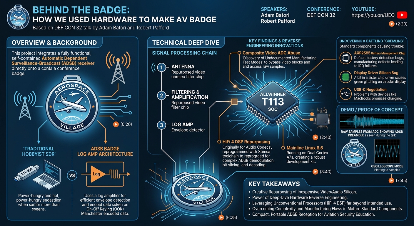
- Composite Video ADC Abuse for RF Signal Digitization: The most significant discovery was the successful exploitation of the Allwinner T113 SoC's composite video Analog-to-Digital Converter (ADC) for digitizing 1090 MHz ADSB signals. Despite lacking a dedicated high-speed RF ADC, the T113's automotive video focus meant it possessed a fast ADC (requiring at least 27 MSPS for composite video baseband). The team discovered and leveraged undocumented manufacturing test modes and registers within the Allwinner chip. These hidden functionalities allowed them to bypass the integrated video processing blocks (H-sync, V-sync, color correction) that would normally prevent access to raw samples, thereby isolating the ADC for direct, high-speed data acquisition. This turned a cheap video chip into a capable RF ADC.
- Repurposing the HiFi 4 DSP for ADSB Demodulation: The Allwinner T113 also features a HiFi 4 DSP, advertised as a third processing core primarily for audio co-processing. The team successfully reprogrammed this DSP, originally designed for audio codecs, to perform the complex demodulation, Manchester decoding, and bit slicing required for ADSB data processing. This involved sourcing the proprietary Xtensa toolchain and vendor-specific IP block (a Verilog blob) to correctly configure the compiler for the exact silicon's vector units and registers, unlocking the DSP's full potential for high-speed signal processing.
- Full Mainline Linux 6.6 Integration: The team achieved the impressive feat of running a full mainline Linux 6.6 kernel on the badge's dual Cortex A7s. This provided a robust, open-source development environment, allowing for easier driver development and application deployment, effectively making the badge a portable Linux development kit.
- Creative RF Front-End Design: Adam Batori, undertaking his first RF project, designed a "zero to triband microwave RF" front-end in just four months. This involved using readily available, inexpensive components, such as a composite video amplifier/anti-aliasing filter chip, to construct the necessary amplification and filtering stages for the 1090 MHz band, demonstrating that sophisticated RF design doesn't always require custom, high-cost components.
- Uncovering and Battling "Gremlins" in Standard Components: The development process highlighted the unexpected challenges posed by seemingly standard components. The team spent considerable time debugging issues with the AXP2585 battery management chip (e.g., incorrect battery detection defaults, MacBook charging issues, manufacturing defects causing IRQ failures) and a specific silicon bug in the display driver that caused the 480x480 circular display to turn green. These experiences underscored that even mature hardware can harbor obscure bugs or manufacturing flaws that demand extensive reverse engineering and debugging efforts, often consuming more development time than the novel, custom-designed parts.
These findings collectively demonstrate a remarkable blend of hardware hacking, software engineering, and relentless debugging, pushing the boundaries of what's possible on a constrained embedded platform like a conference badge.
Technical Deep Dive
▶ Watch: Introducing the log amp architecture for ADSB reception (3:40)
The core technical innovation of the Aerospace Village badge lies in its highly optimized and repurposed signal processing chain for ADSB reception. The journey begins with the raw RF signal and culminates in decoded flight data, leveraging several unconventional design choices.
The ADSB protocol itself operates on the 1090 MHz Mode S downlink. The data is On-Off Keyed (OOK), meaning the presence or absence of an RF carrier signifies a binary state. Furthermore, the data bits are Manchester encoded, where a transition from low to high (or high to low) within a bit period denotes a '1' or '0', providing self-clocking capabilities.
The badge's receive chain employs a log amp architecture, chosen for its power efficiency and suitability for envelope detection compared to a full SDR. The process unfolds as follows:
- Antenna & Initial Amplification: The incoming RF spectrum is captured by the antenna.
- Filtering & Amplification: This raw signal undergoes multiple stages of amplification and filtering. Crucially, very tight 1090 MHz band-pass filters are used to isolate only the specific frequency slice relevant to ADSB. The team ingeniously utilized a cheap, readily available composite video amplifier and anti-aliasing filter chip for this stage. While designed for baseband video signals, its integrated eighth-order Butterworth filter, multiple channels, power amplifiers, and clamp diodes proved highly effective and cost-efficient for the 1090 MHz RF front-end, as composite video components are now considered obsolete and thus inexpensive.
- Envelope Detection: The amplified and filtered signal, representing the logarithmic received RF power, is converted into a linear output voltage by the log amp. This effectively acts as an envelope detector, extracting the amplitude variations (the OOK data) from the high-frequency carrier.
The next critical step is digitizing this analog envelope. Traditional high-performance RF-intended Analog-to-Digital Converters (ADCs) are prohibitively expensive. The badge's Allwinner T113 System-on-Chip (SoC), the main Linux component featuring dual Cortex A7s running at 1.2 GHz, does not natively include an ADC fast enough for ADSB demodulation. However, the T113 is designed for automotive video applications and thus supports composite video input. Composite video baseband signals require ADCs sampling at a minimum of 27 Mega Samples Per Second (MSPS). The T113's block diagram indeed shows an internal ADC for this purpose.
The challenge was that this internal ADC was not directly accessible. It was "wrapped inside a bunch of filters" and hardware blocks designed specifically to demodulate composite video, including Programmable Gain Amplifiers (PGAs), H-sync/V-sync detectors, and color correction filters. This meant the ADC output was not raw samples but "pixels," pre-processed by the video logic, rendering it useless for ADSB. The system would simply report "no video signal" and do nothing.
The breakthrough came through extensive reverse engineering of the Allwinner chip. The team discovered certain undocumented registers that could put the SoC into a "special manufacturing test mode." Silicon manufacturers often include such modes to bypass functional blocks and isolate components like ADCs for performance verification during fabrication. By activating this test mode, the team was able to effectively "bypass out the actual like video, the H sync, V sync blocks," gaining direct access to the true raw samples from the onboard ADC. This allowed them to abuse the video ADC as a standalone, high-speed data converter for the ADSB envelope.
Once digitized, the raw samples are fed into the HiFi 4 DSP integrated within the Allwinner T113. This DSP core, typically marketed as an audio co-processor, was reprogrammed for the computationally intensive tasks of demodulation, Manchester decoding, and ADSB bit slicing. This required a deep dive into the HiFi 4 architecture. Unlike general-purpose CPUs, DSPs are highly specialized for signal processing, often featuring Single Instruction, Multiple Data (SIMD) vectorization units for parallel computation. To fully leverage these capabilities, the team had to acquire the proprietary Xtensa toolchain and the specific vendor IP block (a large Verilog blob describing the exact silicon configuration). This allowed them to compile highly optimized code that matched the chip's specific vector units and register configurations, maximizing the DSP's performance for ADSB processing.
The badge's overall architecture is powered by the dual Cortex A7s running full mainline Linux 6.6. This provided a stable and feature-rich operating environment for managing the various hardware components and running the application logic. The display is a custom-manufactured 480x480 circular display, giving it a distinctive radar-scope or oscilloscope appearance. Storage is handled by 8 gigabytes of eMMC, complemented by 128 megabytes of DDR3 SDRAM. Additional features include integrated GPS and WiFi, adding further connectivity and utility to the badge.
Despite the elegance of these technical solutions, the development process was fraught with "Gremlins." Adam Batori noted that the custom RF, undocumented ADC abuse, and DSP reprogramming were "actually the easiest part." The real challenges came from seemingly standard components. Issues included:
- USBC Complexity: Navigating the intricacies of USB Type-C, including instances where the badge would attempt to charge a connected MacBook instead of being charged itself.
- AXP2585 Battery Management Chip: This chip, a USBC negotiator, battery charger, and Battery Management Unit (BMU) all-in-one, presented numerous bugs. These included incorrect default battery detection leading to instability, and a critical manufacturing defect where a ground pin was improperly soldered, causing voltage drops and intermittent IRQ failures that delayed the project significantly.
- Display Driver Silicon Bug: A three-week debugging effort was spent tracking down a specific bit in a sister chip's driver that, when set, caused the MSB of the green channel on the display to glitch, resulting in a persistent green tint.
These "Gremlins" highlight the immense complexity of modern hardware development, where even well-documented components or manufacturing processes can introduce obscure, time-consuming challenges.
Demo / Proof of Concept
▶ Watch: Leveraging the Allwinner T113 SOC's hidden ADC (6:25)
While the talk itself was delivered under time constraints and did not feature a live, interactive demonstration of the full ADSB reception process in real-time, the speakers clearly articulated and showed evidence of the badge's core functionality as a proof of concept.
The most direct evidence of the successful hardware abuse was a trace pulled directly from a badge with the RF front end attached. This trace, displayed during the talk, showed the ADSB preamble and the start of a data packet being received as raw samples from the onboard ADC. This visually confirmed that their reverse engineering efforts to access the undocumented manufacturing test mode of the Allwinner T113's composite video ADC were successful, and that the ADC was indeed capable of digitizing the ADSB envelope.
Furthermore, the team developed a "cool oscilloscope mode" on the badge itself, which could read directly from the ADC and plot the samples on the custom 480x480 circular display. This functionality served as an invaluable debugging tool during development and also as a visual demonstration of the raw signal acquisition. The culmination of these efforts was a fully operational badge capable of receiving and decoding ADSB signals, providing information like call signs, flight numbers, and altitude to users, effectively demonstrating the feasibility of their ambitious hardware and software integration project. The speakers encouraged attendees who received a badge to tag the Aerospace Village on Twitter to share their experiences and the planes they picked up, implicitly confirming the widespread distribution of functional units.
Defensive Implications
▶ Watch: The "undocumented registers" hack to bypass chip filters (7:45)
While the talk primarily focuses on offensive hardware exploitation and creative engineering, the insights gained have several important defensive implications, particularly for hardware developers, reverse engineers, and those involved in embedded systems security:
- Undocumented Silicon Features are a Double-Edged Sword: The successful repurposing of the Allwinner T113's composite video ADC by accessing undocumented manufacturing test modes highlights that modern SoCs often contain hidden functionalities. While the speakers used this for an innovative, benevolent purpose, malicious actors could potentially exploit such undocumented features for unauthorized access, data exfiltration, or to bypass security mechanisms if these modes are not properly secured or disabled in production devices. Hardware designers should be aware of such hidden capabilities and ensure that all sensitive test modes are permanently locked down or removed in final silicon.
- Supply Chain Vigilance is Paramount: The persistent issues with the AXP2585 battery management chip, particularly the manufacturing defect causing an improperly soldered ground pin, underscore the critical importance of rigorous supply chain scrutiny. Even visually inspected components from reputable manufacturers can harbor subtle defects that lead to system instability, security vulnerabilities (e.g., unexpected power states), or severe operational delays. Organizations should implement comprehensive testing protocols beyond visual inspection, including electrical and functional testing, for critical components.
- Complex Components Introduce Hidden Risks: The challenges faced with USBC negotiation and the AXP2585 demonstrate that integrating complex, multi-functional chips can introduce unforeseen "Gremlins." The sheer complexity of modern standards like USB-C means that even well-implemented solutions can have unexpected interactions. For defenders, this means understanding that the attack surface extends beyond software to the intricate dance of hardware components and their firmware, requiring a holistic approach to system security.
- Repurposing Hardware Can Create Unexpected Attack Vectors: The creative use of a composite video amplifier for RF and an audio DSP for signal processing showcases the potential to repurpose common, cheap components for specialized tasks. While beneficial for innovation, this also implies that attackers might find similar ways to leverage seemingly innocuous hardware for unintended, potentially malicious, functions. Security analysis should consider the full capabilities of all integrated components, not just their advertised uses.
- ADSB Security Landscape: Although not the direct focus of the talk, the core subject matter—ADSB—is inherently an unencrypted and unauthenticated broadcast protocol. The ease with which a sophisticated receiver can be built (as demonstrated by the badge) reinforces that ADSB is susceptible to various attacks, including spoofing (transmitting fake aircraft data) or jamming. While the badge is for reception, the underlying principles of signal processing could be adapted for transmission, highlighting the ongoing need for more robust, authenticated protocols in aviation.
In essence, the talk serves as a powerful reminder that robust security in embedded systems requires a deep understanding of hardware at all levels, from the documented features to the hidden test modes, and an awareness of the potential pitfalls in component integration and manufacturing.
Key Takeaways
- Creative Hardware Repurposing: The badge exemplifies how readily available, inexpensive components (e.g., composite video amplifier, composite video ADC) can be ingeniously repurposed for highly specialized and unintended functions, significantly reducing costs and development time for complex RF projects.
- Power of Reverse Engineering Silicon: Discovering and leveraging undocumented manufacturing test modes and registers within the Allwinner T113 SoC was crucial to bypassing intended video processing and gaining direct access to raw ADC samples, showcasing the profound impact of deep-dive hardware reverse engineering.
- DSP for Unconventional Signal Processing: Reprogramming the HiFi 4 audio DSP for ADSB demodulation, Manchester decoding, and bit slicing demonstrates that specialized processing units can be leveraged far beyond their advertised use cases with the right toolchains and understanding.
- Challenges of Modern Embedded Systems: The project highlighted that "Gremlins" in seemingly standard components like USB-C controllers (AXP2585) and subtle manufacturing defects can pose greater development hurdles and consume more time than the novel, custom-designed aspects of a system.
- Mainline Linux for Embedded Development: Running full mainline Linux 6.6 on the badge's dual Cortex A7s proved to be a robust and efficient approach for managing complex hardware and software, providing a powerful, open-source development kit in a badge form factor.
- Accessible ADSB Reception: The successful integration of a self-contained ADSB receiver onto a conference badge makes advanced aviation tracking technology accessible and tangible for enthusiasts, demonstrating the feasibility of complex signal processing on a compact, power-constrained device.
About the Speaker(s)
Adam Batori is presented as a key figure in the hardware design and RF engineering for the Aerospace Village badge. Notably, the talk highlights that this project marked his first foray into RF design, a feat he accomplished by creating a "full zero to triband microwave RF" system in an impressive four months. His co-speaker playfully refers to him as a "mad lad" for this achievement, underscoring his innovative and determined approach to tackling complex hardware challenges.
Robert Pafford is the co-speaker who collaborated with Adam Batori on this ambitious project. While the transcript does not provide specific details about his background or company, his contributions were integral to the reverse engineering efforts, software development, and debugging of the various "Gremlins" encountered during the badge's creation. Both speakers are associated with the Aerospace Village, indicating their shared passion for aviation security and hardware innovation within the DEF CON community.